Summary
After a
slight scare last week, a meeting at Danchip clarified some issues and made me realise that the error could be worked around. Again, I have had to make concessions with the design and pull back on some ideas that I have wanted to try out on the wick section to improve capillary action. With only a few days to go until I reach the experimental stage (
Tuesday 25th June 2013), this week will be focused on etching the wafers, cutting them and machining the container cover. Then I will need to put it all together for the next stage: filling and sealing the container with working fluid before testing.
To etch...
I had a meeting with
Karen Birkelund
at Danchip which was very useful and allowed me to clarify what exactly
I could achieve with etching considering the time limits and material I have to work
with. She suggested that I could start from scratch and redesign the
photomask (i.e. the layout of the lizard inspired wicks on the wafer)
and create more workable structures. However this could take weeks. My desire has been
to make do with what I have instead of spending more time and money
(DTU's money!) on more material. However, in hindsight, after
the time spent trying to figure out work arounds, it might
have been more productive starting from scratch...c'est la vie!
...or what to etch
It has been confirmed that in fact, the 5 wafers that are
in storage at Danchip have been treated with photoresist and were
not etched. In the plasma etching process, although photoresist
protects certain areas of the wafer, it is still actually being etched away, but at a slower rate to silicon. Depending on the depth of micro
features, it can be necessary to use a thicker photoresist but hopefully in this case, I can avoid this process.
It has been an iterative process where the following etching concepts have been
discussed and abandoned:
- Depth variation laterally across the wick surface - this process has been not tested before at Danchip and it is feared that delicate equipment could be damaged. The application of Kapton tape to the wafer/photoresist surface could allow selective etching of certain areas but might also damage the photoresist when the tape is removed and prevent further etching.
- Wet etch undercut - this would involve further training and although it could be an interesting result (mimicing the lizard more accurately), the creation of undercut channels would make mass manufacture using injection moulding very difficult as removal from the mould would destroy the structures.
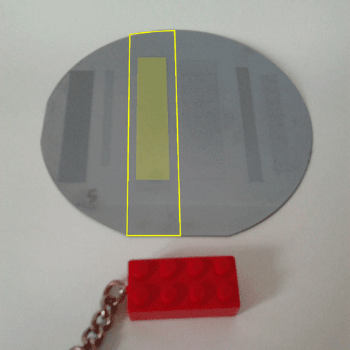
 |
| Cut out (line) and wick area (shaded) | |
 |
| Cut out (line) and wick area (shaded) |
- Create heat pipe wicks from all wafer patterns - handling the wick pattern 'chips' will be difficult due to their small size and once made into a heat pipe container, creating a fill hole for charging and sealing would be very frustrating. Once etching is complete, there will be 5 wafers of different etch
depths
varying from 30 to 150 μm. It has been decided that one wick 'chip'
will be cut from each wafer so that a large enough surface surrounding
the wick structure will be available to join the other container section
(approx. 3 mm). The figure above show which sections will be used
(shaded in red and yellow) and the cut lines are also shown. It will be
necessary to cut out the 'chips'
using a Disco cutting saw such that 5 chips will be available to create 5 heat pipe containers.
They will then be cleaned and taken to the MEK micro fabrication
department (building 427). Karen also suggested that 'blank' extras be made for practising the sealing process. Thanks Karen!
Container design
Last week I spoke to
Jan F. Pedersen
who is the manager of the workshop at the MEK micro fabrication
department (building 427) and was very helpful in his
suggestions about the creation of the cover of the container and how it
could be constructed. He said that it could be possible to machine a piece of plastic into a cover piece using a milling machine with a 1 mm milling tip (I need to confirm what he intends to use but hopefully I can get some hands on experience in this). It could then be glued to the silicon wafer wick section although this would need to be confirmed with the glue manufacturer (Loctite).
The following issues need to be clarified before machining begins:
- Dimensions of container - although most of the dimensions will depend on the wick section area, the height of the container is very important as this will define the vapour section volume during operation. I still need to confirm the pressure drops across the container under different conditions and after reading that Benson et al. had designed flat heat pipes for a maximum pressure of 2 bar (!), my calculations could be well off (I have been thinking about pressures of up to 1 bar). The walls need to be thick enough so the container does not explode and rip off my face during testing (does anyone read this far?). The dimension of the fill hole will also be important but from the papers, 1 mm Ø could be OK but I need to clarify the filling and sealing operation also.
- Material to be milled - the material will be a plastic and should be compatible with the working fluid (water). It should have a coefficient of thermal expansion which is similar to that of silicon so that when in operation, the silicon and cover will expand similarly. Cost is also important as it is hoped that both the cover and wick structure can be created in future using injection moulding so the cheaper the material, the better. The plastic must also have a high thermal conductivity such the heat is transferred through the material at the condenser end.
- Bonding method - Jan suggested I look into the type of glue which could achieve a
hermetically sealed connection under pressures of up to 2 bar,
temperatures of up to 150 °C and also ensure that the glue does not
break up over time (or during bonding) and contaminate the wick cavity. I
emailed Loctite to enquire as to whether they have anything that might
work. Otherwise, another bonding method will be used but as always, time is 'tite'...