
 |
| A selection of the FMHP prototypes |
- Charging and sealing the flat micro heat pipe (FMHP)
- Setting up the equipment for testing the heat transfer capabilities of the FMHP and working out the overall thermal conductivity of the prototypes
- Organise the data and compare to literature
- Putting together the presentation and other stuff that I hope to use for the defence.
Leak tests
I set up a simple leak test to check whether the glue had worked on the prototype FMHP. I set up a test as shown in the image below, sucking out the air, closing the valve and then dipping the end of the tube in water. Opening the valve allowed the water to be sucked through the tube, hence proof that a vacuum existed. However, there could be slow leaks, given time, would relieve the pressure - to be sure, I added an extra layer of sealant. |
| Leak test set up (red areas show potential leak points) |
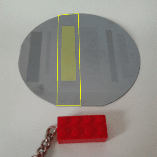
Charging and sealing
Each prototype has an inlet consisting of PTFE tubing with 0.6 mm outer diameter. I am going to attempt to fill/charge the FMHP using a syringe vacuum technique. I will try to evacuate air from the FMHP, then use the internal vacuum in the FMHP to suck in a volume of fluid which should wet the wick section. Then I will crimp shut the PTFE tubing. |
| FMHP charging set up |
The biggest headache thus far has been figuring out how to crimp the FMHP shut. I have tried different methods and tested the crimp by flushing air through and watching for bubbles in a water bath.
 |
| Needle inserted in PTFE tubing and crimped - FAIL. |
- Metal sleeve crimp (as in the last blog post) - this cracked the PTFE tubing and leaked
- Needle crimp - I inserted a steel needle into the PTFE tube (applying glue) and then crimped the steel. I tried a number of crimps, at different angles on the needle but it still leaked. Out of five attempts, one seemed to hold but there was still some air bubbles visible at the outlet. One small bubble seemed to just stick at the end of the needle and I am not sure why this happened.
- Tube bending - I tried to bend the tubing 180 ° and tie the tube in this position but it still leaked.
Testing equipment
Once filled and sealed, I will have FMHP ready for testing. With testing, I will have to apply heat at one end of the FMHP over a small area and then measure the temperature at the other end in order to calculate the over all heat transfer. Practical considerations for the experimental set up will include:- Heater with controllable hot plate that can preferably apply a controlled amount of heat to the Si side of the FMHP. This might involve creating a metal shim 1 cm² in area and surrounding it with insulating material so that heat is focused on a particular region (as in a CPU cooling situation). A thermal insulation paste will be needed to create good contact with the FMHP.
- Thermometers to read the temperatures at different points on the heat pipe. It will be necessary to glue the thermometers which means I need approx 6 per FMHP prototype - 2 at the hot end (evaporator), 2 at the centre (adiabatic region) and 2 at the cold end (condenser). They will have to be glued (i.e. one use only) so I will also need a conductive glue.
- Prof. Larsen suggested a water cooler at the cold end where the inlet and outlet water temperature can be measured (more thermometers). This will involve a structure design which will allow the end of the FMHP fit in securely and be water tight.
a) Melt - PVC can start to soften at 100 °C so I have to keep the temperatures below that which is the case for CPUs which need a safe operating temperature of approx. 85 °C
b) Leak - Will the glue crack and let air in or will the tubing connections leak?
c) Crack under vacuum - Will the combination of heat and pressure crack the plastic? Are there hidden cracks in the Si from my disastrous labelling method (using a glass cutter on Silicon!)
d) WORK!


